本文地址:http://www.moepc.net/?post=4498
原文地址:https://www.anandtech.com/show/12438/the-future-of-silicon-an-exclusive-interview-with-dr-gary-patton-cto-of-globalfoundries
原作者: Ian Cutress
Transcript:Gavin Bonshor
文章很长,写的很易懂,就只提取大家可能关心的部分信息翻译一下了。
In our recent trip to GlobalFoundries Fab 8, its leading edge facility, we managed to spend some time with the C-level executive that controls the future of this part of our industry: Dr. Gary Patton. Gary is the Chief Technology Officer, overseeing all of GlobalFoundries research, development, and fabrication arms, pushing GlobalFoundries towards the next generation of processes for its customers. This includes the current 14nm processes used by AMD and IBM, the new 12nm process for AMD’s 2nd generation of Ryzen CPUs, and the future: multiple generations of 7nm, some of which will have EUV for the critical layers. This list covers Fab 8, but Gary also oversees efforts across the company including the FD-SOI programs (22FDX, 12FDX) and RF related technologies.
Given our recent extensive coverage of GlobalFoundries technology, we were keen to get some prime information about what is coming ahead for GF, especially when it comes to 7nm and EUV, as well as how the company is faring in a foundry business that now only has four on the leading edge.

Some background of Gary Patton: Gary holds multiple Electrical Engineering degrees from UCLA (BS) and Stanford (MS, PhD), and has extensive experience in the semiconductor industry, having held positions at IBM since 1986 and moved over to GlobalFoundries in 2015 as part of the IBM/GF agreement. The leading edge of this industry is where his career focuses on today, pushing into smaller process nodes and new fabrication technologies, as well as what the future holds.
【关于Gary Patton的背景】
Many thanks to Gavin Bonshor for his transcription.
GlobalFoundries and IBM【GF和IBM的合作】
Q1: As you are originally from IBM, when the IBM and GlobalFoundries collaborative agreement happened (IBM fabs to GF, cross-licensing research agreement), the transfer of the personnel and knowledge would have created a massive influx into how GF managed its research. Even though the partnership was extensive before, it is now more vertically integrated. How does that change the perspective of what GlobalFoundries does?
【IBM和GF的合作关系更加密切】
GP: I have done industry analyst briefings fairly frequently over the last two and a half years, and I have a great time with this, because it’s pretty much the same people. When I talked the first time, I had been at GlobalFoundries for 2 weeks! I talked about how this integration was going to be great, it was synergistic, and it was really going to strengthen GlobalFoundries foundry offerings. I talked about better execution, and I like to joke that all the analysts I talked to were polite, they were encouraging, but they were quite skeptical given GlobalFoundries had been struggling for several years. But I had fun coming back and showing them the charts I had shown them originally 2 years earlier and said ‘remember what I said?’ and here’s where we are today.
I think pretty much everyone has acknowledged that GlobalFoundries is executing now. That is not just associated with the acquisition. Sanjay Jha (the CEO) has had laser focus on execution across the entire enterprise from before we came over. The portfolio really works and it’s really synergistic. If you look at leading edge, we licensed 14nm from Samsung and then we forced many enhancements on it. That was great because when you want to bring up a new fab like this, I think the problem they had early on, they tried to bring up the fab and do this leading technology, that’s a tough proposition, and I wouldn’t want that job.
But you know, in effect, I always give credit to Tom (Thomas Caulfield). I said I can do 7nm here (at Fab 8) because we have this great high yielding 14nm manufacturing base that I can do the next node on, right? So it’s great for that, and we brought over the IBM team and integrated them with the 14nm guys, so we have really built a world class team here. I’ve been running R&D for IBM for 8 years, with two and a half here at GlobalFoundries, and I’d say it is the best team that I’ve seen on the field. We have now the horsepower to be able to do our own different technology, take control of our own destiny, and we have great partnerships with AMD, IBM, and our other partners. We’ve been working with those companies for over two years on the definition of our 7nm, and it has really helped us to make sure it is as well targeted for both the mobile hardware and the high performance computing space.
On the subject of the integration, it brought over a lot of extra talent that we needed, Both technology talent as well as design enablement talent which helped bolster our design enablement organization because we’re making a transition. We had historically been a second source player; we’re now really focused on winning first source business. First source business over 7nm is with AMD, IBM, and for our ASIC business, and then our FD-SOI technology is all about winning first source business with differentiated technology.
We brought over IBMs RF business which was the leader, the number 1 in that space, and is very complementary. On all of these technologies we are now offering, we have a roadmap and are offering RF variants on these, for customers that want a logic chip with RF integrated on the same chip. So we got that at 22, we’ve done that on 14, and having that core competency of RF helps strengthen our RF across the enterprise.
【把IBM的RF业务带过来了】
Bringing ASICS over was a huge add, and really bolstered our design enablement capabilities. There are a lot of new players into this market that go do a custom foundry design which is a bit of a challenge at the beginning, but to come in through ASICs where we offer a complete design system they can operate in, it is a much easier path to go and design your own chips. I think you probably know we were number one in SERDES – we have the best SERDES around and for 56Gbps on our 14nm, and we’ll have a really incredible one on 7nm. I don’t know if we’ve announced our SERDES on 7nm, but it will be very important for growth in 5G markets.
On advanced packaging, I think that is really important as well. As you look forward, Moore’s Law is slowing down, and people are looking to integrate more stuff together. We have a strong program in GlobalFoundries on 2.5D and 3D packaging. I had a big program in IBM, and we’ve put those two things together, with our pilot line down in Fishkill where we can do our own development of 2.5D and 3D packages, and we’re seeing a lot of traction now in the marketplace, especially in the high performance computing area where they want to take a silicon interposer and put a lot of different things all on the same package.
IC: What about an embedded bridge?
GP: So I think especially for Artificial Intelligence, these machine learning systems, you want to address the latency issues and bandwidth issues, so you want to get a lot packed all onto one interposer. So we have the 2.5D technology which took a little while to take off, but last year, we started seeing a lot of design wins in our 14nm ASICs which was not just a win for ASICs, but it was also a win for packaging by including our 2.5D technology. We do some of our own production, but we partner with OSATs (Outsourced Semiconductor Assembly and Test providers) for really high volume. For photonics, we picked up all of the IP from IBM on photonics and that is a major program. That actually integrates with our packaging capabilities, looking to do photonics modules, in order to offer a complete solution.
So those were some of the benefits of the IBM acquisition and agreement. I love IBM, which is a great company to work for, but you know, its focus has shifted. It still does systems and that is very important, but to invest in making your own chips when you have other things you need to invest in, it just made a lot of sense to do this deal. GlobalFoundries is going to invest in capacity, and you know the cost of investing in these fabs is becoming pretty large and the IBM volumes are pretty small, but you have to have a certain scale to really get yields and things like that.
Q2: Is IBM one of the most demanding customers in terms of getting the quality of the chip out?
GP: It is a collaboration, and we work really closely with them, and we have also a lot of experience. These are big chips, we’re talking over 700 square millimeters, but we have a lot of experience in how to get it right. For them, it is very important that it is first time right, so we invest a lot upfront in test sites and in analysis to try and identify where the weak points would be in the design. For our first chip, it’s not defect densities so much as systematics that will hurt you.
Q3: Is that primarily a manual process or are there automated tools to help identify the issues?
GP: We definitely use automated tools for that and analysis. But at the end of the day, we put a lot of test structures in place to try to flush out where the weak points might be and where we have to tweak our OPC (optical proximity correction) to tune it so it works. GlobalFoundries has invested in 14nm, is investing in 7nm, and GlobalFoundries is committed to doing a little bit of secret sauce for IBM for what is required for server applications. In exchange IBM keeps doing what they know how to do well, which is research. We have a 10-year research agreement with them that started 2 years ago, and it is definitely a win-win: they get what they need, and they don’t have to invest all this capital and capacity, and we give them the wafers.
Q4: For 14nm, IBM has its own tweaked variant called 14HP. Is this going to be the case for 12nm or 7nm?
GP: We will give them a high performance version on 7nm, and in exchange, they keep helping us with the research, which is becoming pretty challenging.
【IBM在14nm节点用的是自己改良过的14HP,7nm也会有类似的,GF则是帮助研发】

Samsung, 14nm, 12nm, and Half-Nodes【三星,14nm,12nm,以及半节点】
Q5: On the Samsung deal: when it came time for GlobalFoundries to say its custom 14nm process did not work, and GF would have to license somebody else, was that just a factor of resources being split?
GP: This was technically before my time so I don’t know all what went into the decision, but I think it was a smart move. They were trying to bring up this factory (Fab 8) and develop a new technology at the same time and that is very tough. But by having the technology that had been debugged largely, to bring it up the fab, was brilliant. It allowed us to get to work straight away on 14nm. We have of course done extensions on that technology, boosted the performance, and we have a number of customers that want to keep getting improvements in the technology without having to wait for a jump to the next node. Customers want performance kickers as well as some density improvements like in 12LP, which offers about a 10% performance improvement and a 15% circuit density improvement.
【GF自研14nm gg之后转向了从三星授权,GP认为是聪明的举措,14LPP的debug基本已经完成,更容易一些。有些客户不想等到7nm节点,所以有了12LP,性能提升10%,密度提升15%】
Q6: So was 12LP originally called 14+?
GP: No, and we never really had a 14+ per se. We have had what we call BKM, which relates to ‘performance bump’ improvements. I think some companies would call it a plus, you would call it a plus. But 12LP is a completely separate thing, so we had customers who were pushing us for some density improvement and so we did some optimization of the middle line and back-end – it’s not a pure optical shrink. We wanted to do it with minimum disruption to the design IP that had already been developed, for time to market.
【GF从没有把12LP称作14+,如果是Intel可能会这么叫。但12LP和14+是不同的东西,middle line和BEOL有做优化,密度提升,并不是完全的光学制程升级。这样的话已有的设计IP只需要做出最小的改动,能够更快地带入市场。】
【原来预测14+是12LP,现在证实并不是这样。
RR上用到的14LPP高密度版本才是GF的14+工艺。
Intel的14+和14++提升的是晶体管性能,没有密度提升。密度甚至可以说反倒有非常细微的降低,gate pitch有放宽)
GF的12LP基于14LPP平台,提供了MEOL/BEOL、SRAM标准单元库、ground rules的改动,不光有10%的性能提升,实际也有15%的密度提升,和Intel 14+ – hyperscaling的意义并不完全一样。这里原意也只相当于打个比方,不必太过当真。本来Intel的Hyperscaling就是Marketing产物。
如果Intel的14+还能提升15%的密度,那就不会叫这个名了。
Marketing是Marketing,Technology是Technology, 如果把两个东西搞混就不对了。采访的这位是CTO,C ! T ! O ! 不是你们通常会读到的Marketing bullshit。】


Q7: So it’s not a pure optical shrink, so there is a partial optical shrink?
GP: Yes, the middle line and back-end (BEOL) is where we did our tuning.
Q8: So is 12LP in high volume manufacturing now?
GP: It is ramping with Q1 production. We will be ramping through the year.
【12LP正在增产,Q1 量产,持续一整年】
Q9: As far as what we’ve been able to determine, the difference between 14LPP and 12LP is just a difference in going from 9T to 7.5T design, with that tuning. Are there other changes?
GP: Along with the track changes, we also changed the middle and back-end-of-line ground rules. One thing that I think we’re noting is that the industry focuses a lot on pitches, but that’s like having half the story. So much of it is also all the little subtle secondary ground rules.
【除了9T改为7.5T之外,12LP在MEOL/BEOL的设计规则上进行了改进。】
For example, we have a shrink on our 7nm from 14nm that is 0.37x scale. So it’s more than 50% scale at a logic library level. When we first started, we were more like 0.50x or 0.55x and then there was a lot of work with our partners on all the secondary ground rules. How you route the wiring played such a huge role.
【从14nm到7nm – 0.37x倍,高于50%。原本目标是0.5-0.55x,后来和友商合作后,在布线等设计规则上进行了优化。】
At least one of our competitors spends a lot of time talking about the pitches and the things like that, but at the end of the day, a lot of it is how you develop all the rules for the back end and how you develop the routing. We went from 0.50x to 0.37x without changing the pitches. It was all optimization of these secondary ground rules.
For something like 12LP, we try to make it as seamless as possible for our customers. They’ve invested all this money in the platform, but with the minimal investment, they want to be able to get improvements and enhancements because it is taking longer to get from node to node.
【12LP这种制程能让客户在做最小投入的同时,获得性能提升。因为节点和节点间的时间拉长了。】
We will intentionally skip 10nm. I call 10nm more of a ‘half-node’ you know, and there are some people who are very focused on the Christmas season. Therefore they have to get something out and it may not have a great deal of improvement for you.
【跳过10nm是有缘由的。10nm更类似于“半节点”,提升不算很大】
Q10: The mobile industry likes to do that, with the smaller chips. What is your opinion on these half-nodes?
GP: Yeah, and you saw 20nm ended up being a very weak node. It was the end of the road on planar transistors and as a result, you were basically fighting electrostatics. It didn’t have a lot of performance gain, and it didn’t have a lot of density. The same thing has happened with 10nm – I mean if you look at the scaling and the performance, it is a pretty weak node. We want to focus on nodes that will give a very strong value proposition, so we are focusing very hard on 7nm, and making sure for customers jumping from 14nm to 7nm that we are giving them a really significant improvement. So we scaled it. I say simple logic is scaled 0.37x, because we know with these advanced nodes you are adding a lot of complexity.
That is the problem with 10nm, as you’ve added a lot of masks, you’ve got some scaling, but you’ve added a load of mass so when you combine it, the cost improvements are not that great. We’re getting a full node, or greater, of cost improvement if you jump from 14nm to 7nm. You are getting well over a full node on the cost scale, and we’ve got a very substantial performance improvement with the technology.
【比如20nm节点就很差,已经到了planar晶体管的末路。性能不咋地,密度也不咋地。10nm的处境也很类似 – 光看密度和性能,10nm节点的性能提升是很小的。GF专注于更有价值的7nm节点,确保从14nm到7nm能带来显著的性能提升。简单逻辑单元做到了0.37x。】

The Next Generation: 7nm and EUV【下一代:7nm和EUV】
Q11: In the middle of last year, GlobalFoundries announced it was going to offer 3 generations of 7nm, one based on purely DUV/optical and the other 2 using EUV. Is this still the case?
GP: It is maybe a little more complicated than that. On all of our high-level nodes, we will be doing performance boosts, kind of like what we’re doing on 14nm. So you can kind of think of it as if there are two axes: we will be continuing to boost the performance of the offerings, and we expect 7nm, like 14nm, to be a long node – a big node! So we have to have a roadmap where we keep enhancing it. For the two axes, one is performance, and the other is EUV, for cost improvement and density improvement. As we go along, we have plans to boost the performance – but what we will exactly name them is yet to be seen. We will be phasing EUV in, and first drop it in for contact and vias, because that is the low risk path, and you can get away without a pellicle. This improves the cost of the process by reducing the manufacturing steps, and for our customers it means no design rip up. The 2nd phase would be leveraging it to really get a shrink using EUV. We will apply it selectively, kind of like we’re doing with 12.
【会持续改进7nm制程,两把武器:制程性能,和改进成本、密度的EUV。初代降低成本,导入EUV采取低风险方式,只在部分层中采用,减少生产步骤,降低成本,客户不需要修改设计。第二代才是真正的提升密度,也是有选择性的,类似于12LP的路子。】
Q12: So when it comes, the contacts and via replacement using EUV, you already stated the idea is that you want to make that process essentially interchangeable with the fully optical process. But when it comes down to doing something more complex, will that require your partners to essentially recompile with EUV in mind?
GP: There will have to be some interchanges in the libraries, so there is some design rework. So we are working with them right now to define what that rework is – if it is too small, then it is not worth it. If you make it too big, then it becomes too big of a design effort, so we are trying to find that sweet spot with them.
Q13: With EUV still in the process of being brought up, and the way it is with counting masks and pellicle support coming through, is there ever a mentality of 7nm not getting EUV, and that 7nm could end up a purely optical transition? Do you fully expect EUV to come in at 7nm?
GP: I absolutely believe that EUV is here. It’s coming, I absolutely believe it so. As you’ve seen with the machines we are installing in the clean room, we have placed a big bet on it. As Tom (Thomas Caulfield) was saying, it’s a pretty high scale investment. I think if you look at the tool itself, for example, ASML has demonstrated 250W with it. This is pretty repeatable, so I think that it looks in good shape. There are some challenges with the collector availability. They are getting close, I think around 75% availability now is pretty solid, but they have to get to 85%, and they are cranking these tools out. Even with this as a work in progress, there are going to be a lot of tools out on the field, and that is going to also help with improving the performance and control of the tools. The tools we have here are the ultimate tools, the ultimate manufacturing versions.
The lithographic resist is a little bit of a challenge, but we are still trying to optimize that. I don’t see that as a show stopper, as we are managing throughout bring up. I think the real challenge is the masks, and I feel very good about the pellicle process. They have made a lot of progress, and they have shown it can handle 250W. The biggest issue has been that you lose a bit of power – so you’ve done all this work to get to 250W, and then you just lost 20% of that. So it has to go up another 10%, so it’s closer to 90%, in terms of a loss to be viable. For contacts and vias, we can run without pellicles. We have the right inspection infrastructure to manage that, and then bring the pellicles in when they are ready.
One of our competitors took the approach that they are going to go all-in with metal lines, contacts, and have no immersion – just go straight to EUV. Our customers want to tape out this year right? With EUV that is pretty risky, as they want to tape out a product and sell it to end-customers. I’ve said publicly numerous times, I cannot put EUV in the critical path for my customers who want to tape out later this year. We have said we would launch with immersion (a fully optical process) first, and then phase in a EUV once we get comfortable with it and that’s what we’re doing.
I’ve been actually on the same strategy here for 2 years since I came to GlobalFoundries. I launched EUV here, and I said we are not going to put it in a critical path first. We are going to launch with immersion, and contacts/vias are clearly the lowest risk path to get EUV in and to get learning. After that, then you bring it into metal lines with a solid pellicle process. Then the process is not a risk to our customers.
Q14: Will GlobalFoundries 7nm have different processes focused on high performance, on mobile, and on low power?
GP: We use different libraries [in the same process]. Libraries are optimized differently, so we have one that is a 2 fin library, so it is ultra-dense, and another that is a 4 fin library for maximum performance. The other thing we did different to some of the other players is that we built a lot of flexibility into our back end, so where there is high performance computing, there is a place where you’re going to want to run wider lines and they can do that; we have a place where you can put larger vias, and they can do that. So where IR drop is an issue on a critical path, they can do that with the way we designed our back end line.
【2fin的高密度单元库,和4fin的高性能单元库。】
Q15: With the first generation of 7nm, do you expect to be high volume production by the end of the year?
GP: By the end of the year or most likely in early 2019, with a couple of key partners. Our ASIC customers, of which there are quite a few, are also lead users of our 7nm process.
【首代7nm量产时间 – 2018年底前,更可能2019年初,给重要友商。包括ASIC】
Q16: So with the first generation of 7nm, with quad patterning involved, whenever we talk to people involved in semiconductor design, if you mention quad patterning they tend to give an awkward look. As you have seen the semiconductor industry grow, are you fully confident in the quad patterning capabilities?
GP: From where we are applying it, that hasn’t been a big challenge. It does make process longer, which has a knock-on effect when climbing the yield curve, but it has not been one of the major issues.
【四重图案化】
Q17: Does the first generation of 7LP target higher frequency clocks than 14LPP?
GP: Definitely. It is a big performance boost – we quoted around 40%. I don’t know how that exactly will translate into frequency, but I would guess that it should be able to get up in the 5GHz range, I would expect.
【7LP频率提升显著 – 大约40%,应该能到5GHz范围】
Q18: So you would do a custom version of 7LP for IBM, who is currently running 5.2GHz on its 10 core chips – could you also perhaps translate that 40%?
GP: I’m not a system guy so I wouldn’t want to commit IBM to it! But certainly, we are very focused on delivering to IBM the performance they need for the next generation, for power and integration into systems. Some of us have worked with them for many years, so we have a good understanding of what they need.
Q19: In terms of your current manufacturing infrastructure, what more do you need to do to enable optical 7nm?
GP: We have what we need in place here for optical 7nm. You can see we are putting in place the infrastructure needed for EUV, and that includes both in fab as well as in our mask house. We make our own masks, and we are putting that infrastructure in place there.
【首代7nm需要的东西都在准备】

After 7nm【7nm之后】
Q20: Other foundries in the industry have made announcements regarding post their plans to build fabs around post 7nm technologies (5nm, etc.). Is there anything you would like to say on behalf of GlobalFoundries about that?
GP: We are working very hard with our partners in Albany, with IBM, and with Samsung, on technology for what is next. We pushed with them on a research paper last year on 5nm – 5nm with nanosheet/gate-all-around technology, and the first demonstration of that on a chip working or a full block of circuits working. So we have worked there on that, and we have worked on vertical transistors. I believe FinFETs are starting to run out of steam, and I think it looks to me that 5nm could end up being a little bit like 10nm and 20nm – maybe a lot like 20nm. It is kind of the end of the road for device structures, but for some foundries you have to get something out for the Christmas season…
【FF也将走到末路,5nm可能会和20nm的命运一样。】
Q21: So at that point you have to move to gate-all-around?
GP: I think to get a real boost off of 7nm, it is going to take a jump to a new device architecture.
We would like to do what we did with 7nm, which is come out with a full-on node rather than a half-node. Because the design investment for these things, concerning our customers, it is a big design investment to move to a new technology now, and we want to make sure for the customer base we’re interested in, that we’re giving them a substantial improvement in density and in performance.
So are we going to call the next one 5nm? I’m not going to worry ? I’m just going to call it the next node. I can tell you that we will have a significant performance and density improvement.
Q22: Do you/GlobalFoundries care what other semiconductor manufacturers call their processes?
GP: Not really. Our customers know the difference – they get our design kit, they can layout circuits, they know how dense we are. There’s no confusion about what our node is. Our 14nm is very competitive with other industry 14nm and 16nm foundry offerings. Our 7nm, which we know from benchmarking, is extremely competitive with other foundries offerings. We are not talking like the differences are 10%; we are talking about 1 or 2 point differences. Our 12nm, we believe, is very competitive with other 12nm offerings. We think that we are pretty well aligned with the other foundries and we have tried to be consistent to avoid confusion, but you know at the end of the day, our platform customers know what our density is.

Extreme Ultra Violet (EUV) Technology Tools【EUV工具】
Q23: We saw in the fab one EUV machine almost complete and being tuned, with another machine being constructed, and space for 2 more. Given ASMLs ability to produce these machines in small numbers for 2018, when do you expect those 3rd and 4th spots to be occupied?
GP: We haven’t decided yet. I am not worried about getting a tool, if that is your question. They have announced that the machine production output is going to double, and I think that will be true. Even though this is still only a low double-digit number of machines, there are only four companies buying them. We do technically have a third tool that is there in the ASML factory that was bought by GlobalFoundries several years ago. That one just requires to be upgraded, so we have one tool in our pocket if we need to.
【Fab里已经安好了一台EUV光刻机,正在调试;一台正在装配,另外还给两台预留了位置。GF还没决定是否增加光刻机数量,不担心拿不拿的到机器的问题,ASML说产量会翻番,虽然产量也只有两位数,不过买家在全世界只有4个啊。ASML工厂里的确还有第三台GF几年前订的EUV光刻机,只是需要升级。】
Q24: What about development machine in Albany?
GP: That one in Albany can’t be upgraded to a production ready machine, but the one that is sitting in ASML can be upgraded. So at the right time, we’ll either bring that right in and upgrade it here, or upgrade it there first. That will give us a third tool, and then we’ll have to be in the queue for the 4th tool but I’m not too worried about when we can get that. The development tool in Albany acts as a backup for learning, and to be clear, we had the first alpha tool in the industry in our Albany nanotech center. We have been working on EUV for a long time.
So coming back to the original question, I have no doubt in my mind that EUV will be part of 7nm. Absolutely no doubt.
Q5: So with GlobalFoundries third generation of 7nm, using EUV, you expect it to be used extensively?
GP: Yes.
Q26: ASML has quoted that the EUV tool does around 125 wafers an hour. This is a lower throughput than the 14nm tools, so do you not worry about the ability of the tool given that you have plenty of 14nm tools?
GP: Keep in mind that the bar has come down quite a ways for EUV. If we brought it in at 14nm, it would have saved only two lithography steps for each use. At 7nm however, we are talking about replacing three or four DUV masks, for one on EUV. So while the wafers per hour throughput of the EUV tools is not as good as DUV, by replacing 3 masks plus etches and depositions, you remove a whole lot of other steps for an overall speedup.
【ASML称EUV每小时大概125块晶圆,比14nm的光刻机速度更慢,但EUV在7nm上可以用1层掩膜取代3到4个DUV掩膜 – 即便EUV光刻机每小时晶圆输出量不如DUV,考虑到减少的生产步骤,最终速度还是有提升的。】
Q27: With the first two generations of GlobalFoundries 7nm, with the 2nd gen implementing EUV for contacts and vias, would you expect to run these two generations side by side, and do you expect customers to go for one over the other, or do you expect them to migrate to between the two?
GP: I don’t know how that will actually play out. It will depend on cost, but if they see a significant yield boost because we’ve greatly simplified the process, customers may want to migrate over. Yield is one of the expected benefits of EUV, as well as cycle time and a drop in defect density, because you’ve now eliminated a lot of processing steps
Cryptocurrencies and ASICs
Q28: Would you say that your ASIC partners are a mix of old and new customers? New, as in the last couple of years?
GP: Mixed. Some have been our traditional customers for our ASICS business for many years, and there are some new players that can’t be named.
IC: Let’s not beat about the bush, I’m trying to get to cryptocurrency related customers!
GP: I think actually some of the existing players who have graphics chips out there, are being pretty public about their success in the ASIC space. You don’t need 7nm for that.
【Ian这直球…GP只说有AMD的GPU,ASIC不需要7nm】
Q29: We have cryptocurrency mining businesses building chips on other foundries on leading edge nodes, potentially taking up substantial amounts of capacity, perhaps to the detriment of the consumer business. Regardless, it’s still a customer for you if they come to you, but does that factor into your plans at all or you just sell capacity to anybody who needs it?
GP: Obviously we put a high focus on our key partners, but we’re not turning anybody away at this point. For some of that market however, they will be looking at our 22FDX technology, not necessarily 14nm or 7nm. Our 22FDX is manufacturing in Dresden, and Cheng-du, our China factory. 12FDX, the next node, is a high volume, high capacity play for us.

FD-SOI, 22FDX and 12FDX
Q30: Other semiconductor manufacturers haven’t disclosed their FD-SOI plans below 20nm. What makes GlobalFoundries so confident that you can talk about 12FDX?
GP: We have a lot of experience in FD-SOI and we actually did years of work on it in Albany, back in the day actually when I ran IBM’s research. I’ve been in charge of the research center and I had responsibility for Albany. We actually were pursuing both FinFETs and FD-SOI, and at the end of the day, IBM’s focus was on performance at any cost. FinFET is a great technology for that, but if you’re looking for something that is more in the consumer space, you need to balance performance with power and cost, you know FD-SOI is a clear winner. We have 12FDX here and we know we can do the device ? we are actually pretty close to the performance targets already.
We have been doing work on 12FDX here in NY for over a year. We have working devices and they’re not far off the performance target so, and we know how to do 12nm technology obviously since we’re doing 12LPP here. We expect to be taking risk production on the parts early next year (2019), so we are pretty far along with the technology.
【12FDX 2019年初试产】
Q31: Is the escalation of the cost of final manufactured wafers reducing the number of customers to the point of being a concern?
GP: That’s a good question, and it has a two part answer. So part one is what we’ve done here on 7nm: we didn’t make 7nm a marginal node. So companies have just spent a big chunk of money to develop a new technology, you’ve got to give them a value proposition. So we’ve skipped 10m and focused on making sure we have a technology that would give a substantial return for the investment. For part two, the cost of doing these leading edge technology nodes is becoming very prohibitive for a lot of customers, and that is where FD-SOI technology comes in. You’re talking about 40% less masks, a much simpler process – you don’t have all this triple/quadruple patterning with less stringent design rules. It is a much smaller hill to get into the technology, and a much smaller entry cost to prototype. At the end of the day, it is a technology that is really focused on the consumer marketplace
Q32: Can you implement good RF on 22FDX?
GP: We are seeing a tremendous amount of traction. It’s not just the base technology, but you know, we’ve got an RF variant, and people are looking to integrate it all together. We have an ultra-low power version, an ultra-low leakage version, we are going to have millimeter waves, and we are going through the automotive qualifications so it can be used there as well. So really, we have the marketplace by not just focusing on FinFET. Our competitors have only recently woken up and recognized that and they have to come out with their own 22m, FD-SOI technologies, which was a first for us.
IC: I mean it clearly sounds like GlobalFoundries focuses on nodes that will be high volume and suitable for everybody rather than the sort of half nodes.
GP: Most customers have developed all this IP, so that is why the performance boosts, shrinks, integration of RF, automotive qualification of our 14/12nm platform is important. We will also integrate MRAM onto our 22FDX process. That is very big for artificial intelligence. We have integration with our 14nm/12nm platforms with 2.5D and 3D packaging, and we expect these platforms are going to have their variants, but really to be on course for us and for our customers
I did want to make one more core comment at 22FDX: I think one thing that might not be clear is that our 22FDX was specifically optimized for the IoT/mobile/automotive space, from the ground up. Because our competitors had to react, they have tried to take what they have, and tune it for that space. One of our competitors was taking a high performance FinFET and trying to crank it down, while another other was taking planar bulk transistors and struggling past 22nm. We brought up RF on the 22FDX process – one of the things that you can do with our RF that you can’t do with any of these other technologies is that you can stack the transistors. And that is really important for doing integrated power amplifier switches on a chip. Nobody else can beat that, and we are the only one. For IoT, automotive, and mobile, I think FDX is going to be a really winning play and we’ve seen a lot of customers that are looking at it as a path to really differentiate the marketplace.
We just had STMicroelectronics coming up to our FD platform, so we are very excited – they were a partner of ours in the IBM Alliance, and the thing I really like about having ST as a design customer of ours on our FD platform is that they have a tremendous amount of experience, how to do design with body bias. If you’re not familiar with body bias, basically if you go back to the IBM days, we were always pushing partially depleted SOI, so the silicon was thick, the oxide was thick, and it wasn’t fully depleted. But it was all about performance at any cost. So here instead we thinned the silicon so it was fully depleted, just like a FinFET, and we also thinned the oxide so it was very thin so we could actually put a voltage bias underneath the transistor. The end result is that we can crank the performance up and boost it. You can do that at device level, circuit level, you can do that at a block level – and what not? You can get performance when you need it, so on our 22FDX you can easily get 14nm FinFET performance. You can’t get it all the time, but when you need it. With our 12FDX, you can get close to 7nm performance when you need it.
When I say that, I should qualify: you are not going to get that from a big chip. If you are making a big chip, you got tons of wire capacitance, so you are not going to beat a FinFET design. FinFET has huge drive current, so if you’re dealing with smaller chips, wiring capacitance isn’t as a big, but gate capacitance of the transistor is more important. FD-SOI has less gate capacitance than FinFET because you don’t have the gate wrapping around the whole device. So it is ideally suited for smaller chips, I say less than 150 square millimeters.
So with body bias, we’re putting a lot of design IP enablement in place, so our customers can leverage the gains. ST have years of experience doing body bias, and I think they are going to do some incredible products on our FDX platform by leveraging that.
Many thanks to GlobalFoundries and to Gary Patton for his time and insights.
本文地址:http://www.moepc.net/?post=4498
MOEPC.NET节选编译,转载请保留出处。
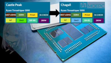
按GP说法, 12nm不是14nm+ . 12nm密度性能双重提升。
14nm+ 是指性能提升,密度不变。
@光辉拉克丝:RR用的就是14+,至少AMD给的材料里是这么写的。
性能没有提升。密度提了,粗略计算大概5%。
GP在文中并没有提到GF自己的14+,你从哪读到的?
这两天忙,没时间上贵站。想不到马文的网站评论区,还挺热闹的。
翻译加料有点多了。
@今天不搞事情:这篇是提取的大意翻译,OK?
没看到哪里有你所说的“加料过多”。
@wangbaisen1990 tsmc做手机SOC还可以,做GPU而且是Vega20这样的大核心,良品率还是有问题,现在实验室可能已经有初样在跑基本测试了(参见去年的金色TITAN泄密事件),离上市还远得很。我个人预测2018Q3之后可能会有准确时间表
@在amd看大门:7nm的vega20面积应该也不大吧
会不会是嵌四块hbm2的难度太大
@在amd看大门:我估计4月份那个台湾大会会有更进一步消息吧
GF 7nm如果没鸽的话
应该能赶在TSMC之前出厂
到时候世界上第一块7nm显卡就是AMD造的了
不知道老黄会怎么应对
希望AMD能在7nm老老实实重新设计一个32核的大DIE
现有EPYC方案,双插居然就有tm八个numa node,内存居然只有12.5%在本地,而且slot内延迟和slot间延迟还差了一个数量级,这做运维的得骂街啊。反正我看买个单槽的做做存储服务器算了,真得干活本代还得xeon。
@xing0999:你要是从chh多蛋哥那里鹦鹉学舌我建议你还是改改,这个水平过不了查重
@在amd看大门:难道这不是事实?
Die间xGMI互联延迟本来就够难看的了,结果slot间还用了更夸张的PCIe
双插的机器赶得上Intel八插
我不知道你对CHH有什么误解,但既然CHH有人提出了相似的观点,说明延迟问题并不是所有人都不关心。
@xing0999:你可能对CHH有误解。
Bullshit spam这次我不说什么。
下次发东西请动动脑子,搞懂之后辨别哪些是真,哪些是胡诌。
尤其是来自某些论坛的内容。
本站欢迎正常讨论,但不欢迎骂街。充满负面情绪,这对讨论问题有百害而无一利。
相关性能问题请拿出实际的系统配置情况,测试项目和性能数字,好让其他人进行测试。
@剧毒术士马文:骂街?我一个脏字没说,贵站的a粉可是动不动就群起而攻之,甚至上前要问候别人母亲呢,您觉得哪方对讨论更有益?
若是贵站容不得一点AMD的负面评论,那我就闭口不谈好了。
@xing0999:已经删掉了那条评论。
两方都有过错
你这样直接往我头上扣帽子可就不对了,什么叫”容不得一点AMD的负面评论”,如果真容不得可会直接像某些论坛那样直接BAN人删评论了,至于是哪些网站,每个人心里应该很清楚。
我说的是有前提的,相关性能问题请拿出实际的系统配置情况,测试项目和性能数字,无论是对哪方都一样。发一大堆毫无意义的牢骚,和骂街大概没什么区别。
如果能提供详细的测试数据,不妨发出来让更多人看到。
@在amd看大门:EPYC号称128pcie
公司运维接tesla跑实时渲染效率还劣于pcie更少的intel机器
查log,大量时间都浪费在了System Coherence上面
这样的胶水128lane也只适合拿去当存储
@xing0999:顺便一提,这软件是少数对AMD友好的,CPU支持SSE3就可以跑(主要做调度),GPU最低兼容到CUDA6.0,饶是这样,大7601还赶不上规格低一大截的xeon gold。
至于AVX类应用?性能只有intel同样核数CPU一半多一点。
VT类?就没几个软件支持AMD-V的。
@在amd看大门:EPYC性价比是高
7601价格只有8180一半,跑CR15和spec2006分数也没落后多少(部分项目还有反超),纸面性能是旗鼓相当的了。
但买服务器又不是只买的硬件,配套的软件设施还有售后服务也是成本,买intel机器还买回来整个intel生态圈,几乎现有软件可以直接兼容,不需要多余的调试。
反观AMD,一堆Intel Optimized软件要么不兼容,要么速度慢一大截(最蛋疼的就是用到Intel VT的软件,压根不支持AMD-V直接报警出错),对AMD系统的优化还要付出大量时间和金钱,最后的综合成本不见得比同规格的intel系统低多少,还要冒着与intel交恶的风险。
AMD不是不好,numa要是花时间优化也不是跑不出高性能,但问题是意义何在,我很高兴AMD能重返高性能CPU市场,但这并不意味着我司就要掏银子去Make AMD Great Again,消费者最终会用脚投票,君不见消费市场还有一大堆跳车ryzen转八代酷睿的吗,只能说AMD还有需要进步的地方。
@xing0999:我只看到oem各种ryzenpro新机子上市,没见什么8100 oem机子
@wangbaisen1990:DIY市场,八代酷睿确实热火朝天,尤其是900元的8400在游戏性能方面一代Ryzen几乎是全线敌不过,不过在Zen+出来后就不好说了。
OEM市场,i社爆出来这么大的漏洞,而且还传出来ceo带头抛售股票的消息,我想OEM老总有点头脑都会暂缓产品的推出,除非想被消费者告到死。Ryzen趁这个真空期可以大杀四方,就看AMD动作快不快了。
@xing0999:套用我导师的一句话“我的审稿建议由原作者采纳,你可以把复印开销发票给我”
@在amd看大门:好的,如果贵站真的容不得一点AMD的负面言论,那我就噤声好了。
@xing0999:生态问题我同意,延迟问题我同意,说不好听点Intel现在阶段就是让客户花钱买方便,AMD现阶段就是低价卖口碑,努力补齐生态。不是所有东西都要用avx512,epyc有他更加擅长的领域,但是被Intel教育的地方也有。一个产品刚出来就赶上Intel好多年的产品线积累本身就不现实,特别是linux领域的大量软件编译优化方面确实是需要人力物力和时间来弥补。amd疲软了这么久,不说其他光编译器这块的优化就一定没有Intel来的深厚。从ryzen转八代酷睿,这个问题其实不是八代当年不好,更不是ryzen比Intel优秀很多,只是因为售价,Intel的天价不是谁都能接受的,但是Intel调整了售价之后,就都一样了,消费者当然会选择有了多年口碑的Intel,而且Intel对分销商的补贴是amd的n倍也是事实,卖家乐意卖买家乐意买仅此而已。你的语气中太多的屁股决定脑袋的思路倾向,不好,希望不要引战。
@xing0999:优化都不是一天两天的事,得一点点积累。无非就是人,钱和时间。
先学会走,再学着跑。有了产品,才能有市场,有了市场,才能有利润,有了利润,才会有更好的产品。
naples的使命不是一上来就大杀四方,玩好1p/2p的部分市场就算功德圆满了,后面的任务自然还有rome/milan来完成。
另外,rome的numa node不会像naples这么多了
@xing0999:WTF?
@xing0999:Chh最新的骂街
zen2 16核要是能跑5GHZ爽歪歪啊
intel hedt平台绝大部分产品都可以淘汰了
@theLastWish:想多了
Intel每年给晶圆厂投多少钱?AMD投多少钱?
这东西有投资才有产出,以GF的尿性,能不延期对AMD就是最大的慰藉了。
@xing0999:人家官方介绍写的达到5ghz啊不是我瞎钦定的
牙膏厂那工艺渐渐吹不动了,差距在被缩小
@theLastWish:Intel工艺吹不动?
TSMC借手机soc东风正在快速追赶,但人家也不敢吹自家工艺就比intel优秀云云。
GF这家坑了AMD无数次的公司,自家的7nm PPT,也只敢吹性能和Intel的10nm差不多(好像是foundry best-in-class和友商对比那张),而且还没有保证过量产时间。
@xing0999:intel在14nm上压榨太多,导致10nm甚至10nm+都不能在性能上战胜末代14nm制程,这可不是我拍脑袋瞎编的,这可是intel官方PPT都承认的事实。
我可不是说intel工艺不行了,民用行业intel工艺还是当之无愧老大,不过22nm前期还是一家独大,现在tsmc、gf、三星、ibm都在制程上领先一步,吹吹水分也比过去强多了
@xing0999:这文章里GP自己也在说“I don’t know how that exactly will translate into frequency, but I would guess that it should be able to get up in the 5GHz range, I would expect.”
@theLastWish:根据目前透露出来的消息是可以量产 但是性能并没有想象的乐观
@NiceMing:4.5基本盘也行
@theLastWish:不用等7nm,现有的12nm都可以跑4.5了
以我之见,AMD真应用fdx做一批cpu和显卡。超低功耗啊。
7nm最早18年底?
那么苏妈不是说下半年要出7nm vega么?
@wangbaisen1990:AMD 在7纳米节点会同时使用女朋友和台漏电的制成
@桜月:难道说台积电7nm节点速度比三星/GF快一些?
@桜月:这样啊,不过这俩的7nm是一套工艺嘛?
@wangbaisen1990:这里asic是指CPU吧?
@amdfan:矿机
@剧毒术士马文:好像22nm/14nm/7nm这种工艺重大节点都是拿这种代工asic芯片试水…
@wangbaisen1990:纸面发布,和老黄发布gX100大核心时一样,设计上就是Vega10加挂fp64单元
@在amd看大门:去年一整年苏妈发布的东西还是按照预计时间点来的,包括今年的2200g/2400g也是一样的
@wangbaisen1990:稳的
@樱:苏妈去年的表现还是很稳的,虽然2500u和2700u的轻薄本国内上市的确有点耽搁……但是这种都习惯了,毕竟hp和dell的轻薄本也没有全球同步上市(尤其是狗逼hp,妈的生产基地就在大重庆)
@wangbaisen1990:问题是苏妈也没确定发布就能拿到现货,到时候拿几块es做演示还是很有可能的
@在amd看大门:台积电进度还好吧?